Description:
A switch is the only input device in the circuit simulation, it does not have any input signals.
You can change the state of a switch by toggling the key.
Usage:
Switch coord output_signal 'toggle_key' init_state;
Switch "label" coord output_signal 'toggle_key' init_state;
Parameters:
label - give Switch component a unique name. (optional)
coord - coordinate of the component.
output_signal - output signal of the switch.
toggle_key - key on keyboard used to toggle the switch, one single character, case sensitive.
init_state - initial state (ONE or ZERO or 0 or 1 ).
Example:
										Switch ab a1 '1' ZERO;

										Switch ab a2 '2' ONE;

										Switch ab a3 '3' 0;

										Switch ab a4 '4' 1;

										Probe ac a1;
										Probe ac a2;
										Probe ac a3;
										Probe ac a4;
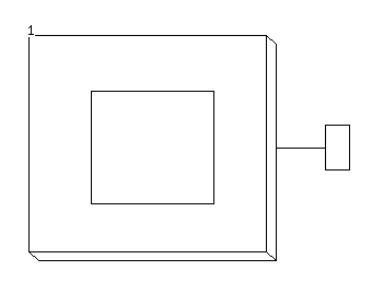
ZERO Signal Output
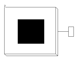
ONE Signal Output
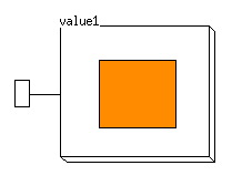
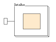
Description:
A probe is the output device in a circuit simulation.
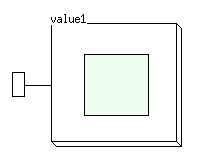
A unfilled circle represents the low (ZERO or 0) value.
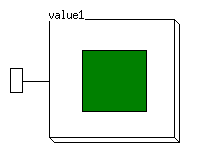
A filled circle represents the high (ONE or 1) value.
The signal name will be displayed at upper left corner of each Probe component.
Warning: DO NOT use a Probe component inside a self-defined component!
Usage:
Probe coord input_signal;
Probe "label" coord input_signal;
Parameters:
label - signal name will be used for labeling (optional)
coord - coordinate of the component.
input_signal(s) - one signal or a group of signals.
Example 1:
											Switch aa a2 '1' ZERO;

											Switch ca a1 '2' ZERO;

											Switch da a0 '3' ZERO;

											Probe ac a2 a1 a0;
Example 2:
											Switch aa a2 '1' ZERO;

											Switch ca a1 '2' ZERO;

											Switch da a0 '3' ZERO;

											Probe ac a2;

											Probe ad a1;

											Probe ae a0;
Example 3:
											Switch aa a[2] '1' ZERO;

											Switch ca a[1] '2' ZERO;

											Switch da a[0] '3' ZERO;

											Probe ac a;
Low signal -- ZERO
High signal -- ONE
XXX signal -- signal in transition
UNINITIALIZED signal
Description:
Same as Probe but display a group of signal horizontally.
Warning: do NOT use a ProbeH component inside a self-defined component
Example 1:
											Switch aa x 'a' ZERO;

											Switch ba y 'b' ONE;

											Switch ca z 'c' ONE;

											ProbeH ac x y z;
Example 2:
											Switch aa x[2] 'a' ZERO;

											Switch ba x[1] 'b' ONE;

											Switch ca x[0] 'c' ONE;

											ProbeH ac x;
Description:
Same as Probe but display a group of signal vertically in a single Probe.
Warning: do NOT use a ProbeByte component inside a self-defined component.
Example 1:
											Switch "my_input" aa R[7] '1' ZERO;

											Switch "my-input" aa R[6] '2' ZERO;

											Switch "myswitch" aa R[5] '3' ZERO;

											Switch "A" aa R[4] '4' ZERO;

											Switch "11" ba R[3] '5' ZERO;

											Switch ba R[2] '6' ZERO;

											Switch ba R[1] '7' ZERO;

											Switch ba R[0] '8' ZERO;

											ProbeByte ac-bc R;
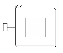
ProbeByte
Description:
Same as Probe but display a group of signal horizontally in a single Probe.
Warning: do NOT use a ProbeByteH component inside a self-defined component.
Example 1:
											Switch ea S[7] 'q' ZERO;

											Switch ea S[6] 'w' ZERO;

											Switch ea S[5] 'e' ZERO;

											Switch ea S[4] 'r' ZERO;

											Switch fa S[3] 't' ZERO;

											Switch fa S[2] 'y' ZERO;

											Switch fa S[1] 'u' ZERO;

											Switch fa S[0] 'i' ZERO;

											ProbeByteH "test111" eb-fc S;
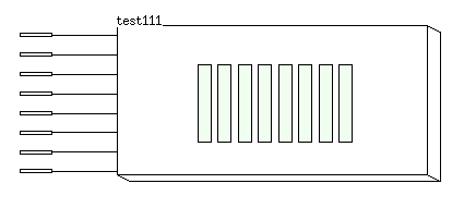
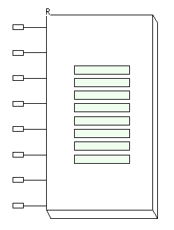
ProbeByteH
Description:
An And-gate is a circuit that performs the AND function in hardware (circuitry).
You can have multiple input signals to the And-gate, the output signal is equal to the And-function of all the input signals.
Usage:
And coord input_signals output_signal;
Parameters:
coord - coordinate of the component.
input_signals - input signal of the And-gate
output_signal - output signal of the And-gate
Example:
And ab s_0 s_1 s_2 s_3 out;
| A | B | OUTPUT |
|---|---|---|
| 0 | 0 | 0 |
| 0 | 1 | 0 |
| 1 | 0 | 0 |
| 1 | 1 | 1 |
Usage:
Nand coord input_signals output_signal;
Parameters:
coord - coordinate of the component.
input_signals - input signal of the Nand-gate
output_signal - output signal of the Nand-gate
Example:
Nand ab s_0 s_1 s_2 s_3 out;
| A | B | OUTPUT |
|---|---|---|
| 0 | 0 | 1 |
| 0 | 1 | 1 |
| 1 | 0 | 1 |
| 1 | 1 | 0 |
Usage:
Or coord input_signals output_signal;
Parameters:
coord - coordinate of the component.
input_signals - input signal of the Or-gate
output_signal - output signal of the Or-gate
Example:
Or ab s_0 s_1 s_2 s_3 out;
| A | B | OUTPUT |
|---|---|---|
| 0 | 0 | 0 |
| 0 | 1 | 1 |
| 1 | 0 | 1 |
| 1 | 1 | 1 |
Usage:
Nor coord input_signals output_signal;
Parameters:
coord - coordinate of the component.
input_signals - input signal of the Nor-gate
output_signal - output signal of the Nor-gate
Example:
Nor ab s_0 s_1 s_2 s_3 out;
| A | B | OUTPUT |
|---|---|---|
| 0 | 0 | 1 |
| 0 | 1 | 0 |
| 1 | 0 | 0 |
| 1 | 1 | 0 |
Usage:
Xor coord input_signals output_signal;
Parameters:
coord - coordinate of the component.
input_signals - input signal of the Xor-gate
output_signal - output signal of the Xor-gate
Example:
Xor ab s_0 s_1 s_2 s_3 out;
| A | B | OUTPUT |
|---|---|---|
| 0 | 0 | 0 |
| 0 | 1 | 1 |
| 1 | 0 | 1 |
| 1 | 1 | 0 |
Usage:
Xnor coord input_signals output_signal;
Parameters:
coord - coordinate of the component.
input_signals - input signal of the Xnor-gate
output_signal - output signal of the Xnor-gate
Example:
Xnor ab s_0 s_1 s_2 s_3 out;
| A | B | OUTPUT |
|---|---|---|
| 0 | 0 | 1 |
| 0 | 1 | 0 |
| 1 | 0 | 0 |
| 1 | 1 | 1 |
Usage:
Not coord input_signal output_signal;
Not coord input_signal(s) | output_signal(s);
Parameters:
coord - coordinate of the component.
input_signal(s) - input signal(s) of the Not-gate
output_signal(s) - output signal(s) of the Not-gate
Example 1:
											Switch aa a '1' ZERO;

											Not dd a z;

											Probe ac z;
Example 2:
											Switch aa a2 '1' ZERO;

											Switch ca a1 '2' ZERO;

											Switch da a0 '3' ZERO;

											Not dd a2 a1 a0 | x y z;

											Probe ac x y z;
Example 3:
											Switch aa a[2] '1' ZERO;

											Switch ca a[1] '2' ZERO;

											Switch da a[0] '3' ZERO;

											Not dd a | x y z;

											Probe ac x y z;
| input_signal | output_signal |
|---|---|
| 0 | 1 |
| 1 | 0 |
Description:
Decoder is a generic form of decoder that allows decoding n inputs to 2n outputs.
If enable = ZERO, then all output signals are equal to ZERO, if enable = ONE, the control signals will make exactly one selection.
Usage:
Dec coord enable inputs | outputs;
Parameters:
coord - coordinate of the component.
enable - one input signal, ONE or ZERO or 1 or 0.
inputs - n input signals(control signals).
outputs - 2n output signals.
Example: 2x4 decoder
										Switch fa c1 'b' ZERO;

										Switch ga c0 'a' ZERO;

										Switch ia enable 'z' ZERO;

										Dec ab-db enable c1 c0 | o3 o2 o1 o0;

										Probe ac o3;

										Probe bc o2;

										Probe cc o1;

										Probe dc o0;
| A | B | D0 | D1 | D2 | D3 |
|---|---|---|---|---|---|
| 0 | 0 | 1 | 0 | 0 | 0 |
| 0 | 1 | 0 | 1 | 0 | 0 |
| 1 | 0 | 0 | 0 | 1 | 0 |
| 1 | 1 | 0 | 0 | 0 | 1 |
Description:
The D-flipflop in logic-sim is a one-bit memory circuit with 2 extra controls.
reset=1 force Dff output to 0.
set=1 force Dff output to 1.
reset=0 AND set=0 Operate like a normal Dff.
Usage:
Dff coord set input clock reset output;
Parameters:
coord - coordinate of the component.
set - ONE or ZERO.
input - one input signal.
clock - one input signal.
reset - ONE or ZERO.
output - one output signal.
Example:
										Switch 2a sw_1 'a' ONE;

										Switch 3a sw_2 's' ONE;

										Dff 2b ZERO sw_1 sw_2 ZERO q;

										Probe 2c q;
| SET | RESET | D | CLK | OUTPUT |
|---|---|---|---|---|
| 0 | 1 | - | - | 0 |
| 1 | 0 | - | - | 1 |
| 1 | 1 | - | - | X |
| 0 | 0 | 1 | 1 | |
| 0 | 0 | 0 | 0 |
Description:
This is a variable-width register. When the enable signal goes high, the current inputs are latched in the Register at the raising edge of write signal.
Usage:
Reg coord enable write inputs | outputs;
Parameters:
coord - coordinate of the component.
enable - ZERO or ONE.
write - ZERO or ONE.
inputs - n input signals
outputs - n output signals
Example:
								Switch aa d[7] '7' ZERO;

								Switch ba d[6] '6' ZERO;

								Switch ca d[5] '5' ZERO;

								Switch da d[4] '4' ZERO;

								Switch ea d[3] '3' ZERO;

								Switch fa d[2] '2' ZERO;

								Switch ga d[1] '1' ZERO;

								Switch ha d[0] '0' ZERO;

								Switch jb enable 'a' ZERO;

								Switch jc wr 'b' ZERO;

								Reg ab-hb enable wr d[7..0] | o[7..0];

								Probe ad-hd o;
Description:
The Mux component is a multiplexer that provides selection among m words, each n bits long. The number of words, m, must be a power of two.
The input selection must be done using log2(m) signal lines. There will be one output word that is n bits long.
Usage:
Mux coord controls | inputs | outputs;
Parameters:
coord - coordinate of the component.
controls - signal length must be log2(# of inputs)
inputs - signal length must be n*2(# of controls), Mux will group bit signal automatically
output - one output signal that is n bits long.
Example 1:
								Switch aa i[3] '3' ZERO;

								Switch ba i[2] '2' ZERO;

								Switch ca i[1] '1' ZERO;

								Switch da i[0] '0' ZERO;

								Switch jb control1 'a' ZERO;

								Switch jc control2 's' ZERO;

								Mux ab-hb control2 control1 | i[3..0] | o;

								Probe ad-hd o;
Example 2:
								Switch aa i[7] '7' ZERO;

								Switch ba i[6] '6' ZERO;

								Switch ca i[5] '5' ZERO;

								Switch da i[4] '4' ZERO;

								Switch ea i[3] '3' ZERO;

								Switch fa i[2] '2' ZERO;

								Switch ga i[1] '1' ZERO;

								Switch ha i[0] '0' ZERO;

								Switch jb control1 'a' ZERO;

								Switch jc control0 's' ZERO;

								Mux ab-hb control1 control0 | i[7..6] i[5..4] i[3..2] i[1..0] | o[1..0];

								Probe ad-hd o;
Example 3:
								Switch aa i7 '7' ZERO;

								Switch ba i6 '6' ZERO;

								Switch ca i5 '5' ZERO;

								Switch da i4 '4' ZERO;

								Switch ea i3 '3' ZERO;

								Switch fa i2 '2' ZERO;

								Switch ga i1 '1' ZERO;

								Switch ha i0 '0' ZERO;

								Switch jb control1 'a' ZERO;

								Switch jc control0 's' ZERO;

								Mux ab-hb control1 control0 | i7 i6 i5 i4 i3 i2 i1 i0 | o[1..0];

								Probe ad-hd o;
Description:
A read-only memory computer memory that contains a set of binary value which cannot be changed.
Usage:
Rom coord address | outputs | rom_content;
Parameters:
coord - coordinate of the component.
address - address signals
outputs - the output signals of the ROM
rom_content - Byte array used to store the values of the ROM entries.
Example 1:
								Switch fa addr[2] '2' ZERO;

								Switch fb addr[1] '1' ZERO;

								Switch fc addr[0] '0' ZERO;

								Rom bb-db addr | out[15..0] |

									0xAA 0xAA

									0xF0 0xF0

									0x33 0x33

									0xCC 0xCC

									0x0F 0x0F

									0xFF 0xFF

									0x00 0x01

									0x80 0x00;

								ProbeH aa-ad out;
Example 2:
								Switch fa addr[2] '2' ZERO;

								Switch fb addr[1] '1' ZERO;

								Switch fc addr[0] '0' ZERO;

								Rom bb-db addr | out[15..0] |

									0b10101010 0b10101010

									0b11110000 0b11110000

									0b00110011 0b00110011

									0b11001100 0b11001100

									0b00001111 0b00001111

									0b11111111 0b11111111

									0b00000000 0b00000001

									0b10000000 0b00000000;

								ProbeH aa-ad out;
Example 3:
								Switch fa addr[1] '1' ZERO;

								Switch fb addr[0] '0' ZERO;

								Rom bb-db addr[1..0] | out[15..0] |

									0b10101010 0b10101010

									0b11110000 0b11110000

									0b00110011 0b00110011

									0b11001100 0b11001100;

								ProbeH aa-ad out;
Example 4:
								Switch fa addr[1] '1' ZERO;

								Switch fb addr[0] '0' ZERO;

								Rom bb-db addr[1] addr[0] | out[7..0] |

									0b10101010

									0b11110000

									0b00110011

									0b11001100;

								ProbeH aa-ad out;
Description:
Tri-state-buffer has two input and one output signal. The inputs are buffered to the output under control of the last input.
When the control line is low, the buffer output will be in the high-impedance state. When the control line is high,
the output will follow the input.
Usage:
Tsb coord input control output;
Parameters:
coord - coordinate of the component.
input - one input signal.
control - one control signal.
output - one output signal.
Example:
								Switch 1a input1 '0' ZERO;

								Switch 3a control1 '1' ZERO;

								Tsb 2b input1 control1 output1;

								Probe 2c output1;
Description:
Random-access memory is a form of computer data storage that stores data and machine code currently being used.
m words by n bits. m = 2(# of address bits)
Usage:
Ram coord enable write inputs | address | outputs;
Parameters:
coord - coordinate of the component.
enable - enable state (ONE or ZERO).
write - write state (ONE or ZERO)
inputs - n bits signal
address - address signals
outputs - one n bits signal.
Example:
								Switch aa inputs[7] '1' ZERO;

								Switch aa inputs[6] '2' ZERO;

								Switch ba inputs[5] '3' ZERO;

								Switch ba inputs[4] '4' ZERO;

								Switch ca inputs[3] '5' ZERO;

								Switch ca inputs[2] '6' ZERO;

								Switch da inputs[1] '7' ZERO;

								Switch da inputs[0] '8' ZERO;

								Switch fa addr[5] 'q' ZERO;

								Switch fa addr[4] 'w' ZERO;

								Switch ga addr[3] 'e' ZERO;

								Switch ga addr[2] 'r' ZERO;

								Switch ha addr[1] 't' ZERO;

								Switch ha addr[0] 'y' ZERO;

								Switch ja write 'a' ZERO;

								Switch ja enable 'b' ZERO;

								Ram db-gb enable write inputs | addr | o[7..0];

								Probe ad-hd o;