Sequential circuits - such as the D-latch - have active and inactive periods.
The output of a circuit will not change during the inactive period. |
is active during the time that the Write signal is 1.
You can try this hands on with the following circuit file: click here
- Toggle key 3 so that the Write signal is 1
- Then toggle key 2 repeatedly. This changes the input of the D-latch.
- You will see the D-latch output change along with the input....
- Active state: the output "follows" the input, i.e., the output changes when the input changes.
- Inactive state: the output does not follows the input, i.e., the output remains unchange no matter what happens to the input.
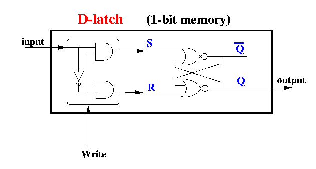
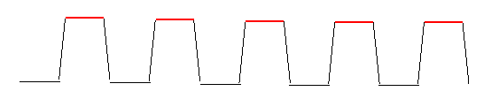
The D-latch in the above figure is active when the write signal (clock) is 1.
In other words: a latch is active when the write signal (clock) is at a certain level (1 or 0)
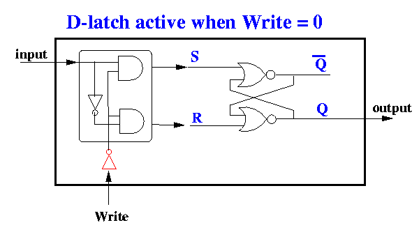
You saw that the following D-latch is level-active for Write = 1
It is very easy to make a D-latch that is level-active for Write = 0, just insert a NOT gate before the Write signal:
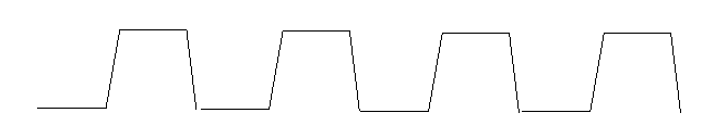
A clock is basically a pacing device and emits a regular pattern or square wave, that looks like this:
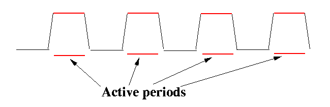
From this figure, one would clear see why latches are called "level-active" devices - the are active when the clock (write signal) is leveled...
To ensure that the correct value is captured, the input value must be kept stable (constant) as long as he Write signal is equal to 1, because otherwise, the circuit cannot ensure (guarantee) that the intented value is captured.
(This may be analogous to a situation when you have exactly 1 min to make up your mind to buy something or not. If you keep changing your mind (yes, no, yes, no, etc) within that minute, it is possible for the system to record a wrong decision. On the other hand, if you keep saying "yes" all the time for the whole minute, there is no way the system will record a wrong answer.)
The fact is: the longer the CPU must keep the signal constant, the longer it takes to complete a CPU cycle and the slower the CPU will run.
You will get a faster CPU if the register has a faster write time, i.e., a shorter active period.
You can a shorter active period by shortening the clock period:
Recall that a memory device is active if the output changes then the input is changed.
An edge-active device is active during the period when the clock changes from 0 -> 1 or from 0 -> 1.
For example, the following figure shows the active period of an edge-active device:
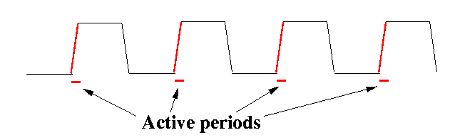
You can clearly see that such a device is has a much shorter active period. These memory elements are much faster than D-latch memories.
Consider the following circuit (which is called a D-flipflop):
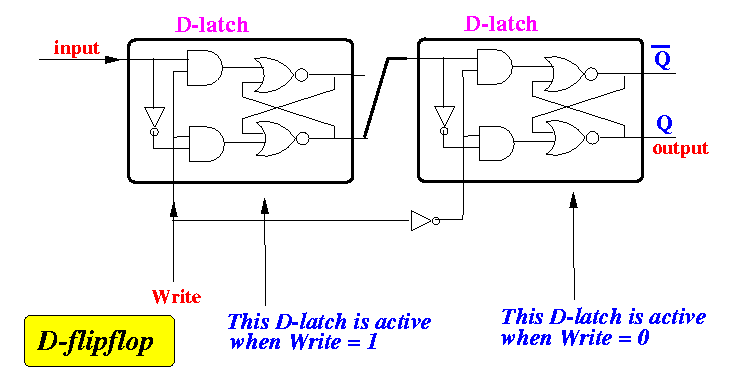
If you look closely, you can see it consists of 2 D-latches. The first D-latch is active when the Write (clock) signal is 1 and the second D-latch is active when the Write (clock) signal is 0. The Q-output of the first D-latch is used as input to the second D-latch.
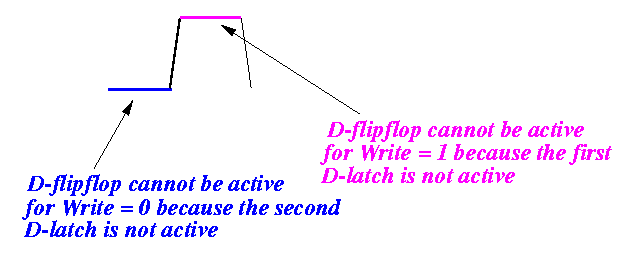
So one can conclude that the D-flipflop cannot be a level-active device...
- Use key 1 to toggle the clock to 0 or 1.
- While clock = 0, use key 0 to change the input continuously. The output remains unchanged.
- While clock = 1, change the input continuously again. The output also remains unchanged.
- The first circuit is a cascaded series of D-flipflips:
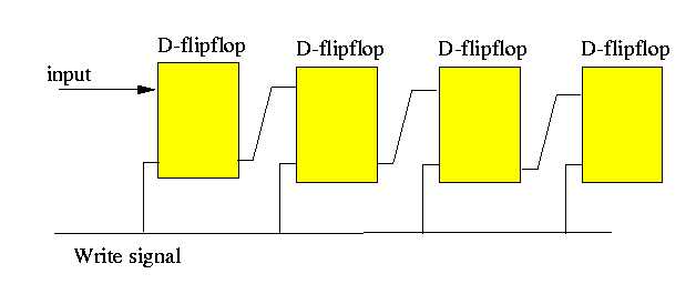
Due to the immensely short write period, each D-flipflop will capture (and store) the current value of its preceeding register and the result is shifting 1 bit for every clock signal.
You can experiment with this circuit with the following logic-sim circuit file: click here. The circuit has been shown in class....
- If we replace the D-flipflops with D-latches, the behaviour is completely
different.
Because the D-latches are level-active, the input signal will
have the time to reach the output of the first D-latch and
immediately enter the input of the second D-latch and changes
the output of the second D-latch.
A few nano-second later, the output of the second D-latch is changed
which will immediately change the input of the 3rd D-latch, and so on.
So the result is: after a (very short time, several 100s nano seconds),
all outputs are changed - because all D-latches remain active for
the entire duration of the period when the Write signal = 1.
You can also experiment this with another logic-sim circuit file: click here. The circuit has also been shown in class....