
- Address bus: used to carry the address of a device.
Each device in the computer is uniquely identified
by a number (address). So each component (memory, and IO devices)
of a computer has a number akin to a Social Security Number...
- Data bus: used to transfer the data (information) between
2 devices in the computer.
- Control bus: contain many signals, among others are
- R/W: the Read vs Write indicator signal. When R/W = 1, the CPU wants to perform a READ operation, and when R/W = 0, the CPU wants to perform a WRITE operation.
- MEM: the memory vs IO device indicator signal. When MEM = 1, the CPU wants to perform an operation with the memory, and when MEM = 0, the CPU wants to perform an operation with an IO device. (in either case, the address on the address bus will indicate the exact memory location or IO device that the operation will be performed on...)
Make sure you realise that in a WRITE operation:
- The CPU signals the write operation to memory by setting MEM = 1 and R/W = 0.
- The CPU provides the data on the data bus
- The data is written to D-flipflops by connecting the data from the data bus to the inputs of the D-flipflops
The following figure show the wiring diagram of a (partial) memory circuit for writing:
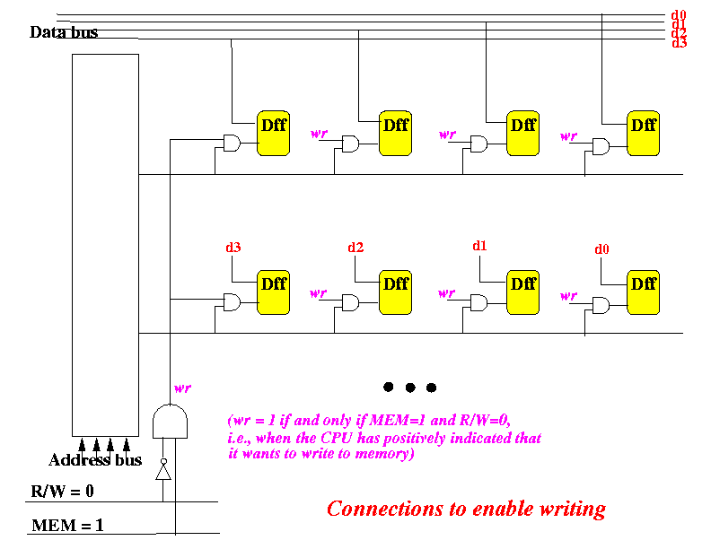
- Each row of D-flipflops is written all at once.
- The row of D-flipflops is selected by the address on the address bus.
- Although the data bus are connected to all D-flipflops, only the D-flipflops in the selected row will be updated.
- The circuitry using the signals R/W and MEM makes sure that a write (or clock) signal is generate only when MEM = 1 and R/W = 0.
Make sure you realise that in a READ operation:
- The CPU signals the write operation to memory by setting MEM = 1 and R/W = 0.
- The memory provides the data on the data bus (for CPU to read)
- The data is taken from the outputs of D-flipflops in the memory by connecting the outputs of the D-flipflops to the data bus. This connection must be made through tri-state-buffers for the reason that we studied before (and too long to write).
The following figure show the complete wiring diagram of a memory circuit for reading and writing. The additional circuitry needed for reading is given in blue:
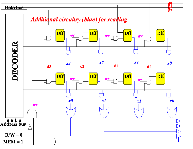
- The output of the DECODER is used to "filter" the outputs of the D-flipflops. All the blue AND-gates will output ZERO, except the row of AND-gates that has been selected by the DECODER.
- The output of the blue OR-gates at the bottom will then equal to the outputs of the selected row of AND-gates (because (x OR 0 OR 0 OR 0 Or .... = x).
- The output of the OR-gates are connected through tri-state-buffers to the data bus.
- The AND-circuit using MEM and R/W input ensures that the tri-state-buffers are only turned on when MEM = 1 and R/W = 1, i.e., only when the CPU wants to READ the memory.
- Immediately after you start the circuit, type "I" and then "r" to hide the connections....
- Keys 1,2,3,4 are used to set a 4-bit value that can be loaded into a CPU register (the CPU register are the Dff right under the switches 1,2,3,4.
- Key 0 is used to load the values in the switches 1, 2, 3, 4 into the Dff of the CPU register.
- Key 5 is write signal of the Dff of the CPU register. Make sure switch 0 is ZERO before you write CPU register, because siwtch 0 is a "FORCE" load operation and has a higher priority than the write signal (yes, we are using a special kind of Dff !)
- Keys 7,6 are the "address bus" signals and select one of the 4 "bytes" in the memory.
- Key 8 is the R/W signal
- Key 9 is the MEM signal
- Try repeat the demo I shown in class....