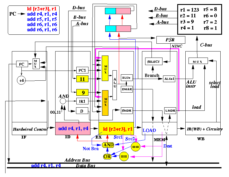
Through additional data forwarding circuitry, we aim to make the value in LMDR avaliable to the EX stage (where the value is need to execute the ADD (or another ALU) instruction.
Because the value in the LMDR will be used to update the register in the next CPU cycle, we do not need to retain the value using additional registers - so there is no need to add forwarding registers.
We only need to feed the LMDR value back to the EX stage and add "intelligent selection" hardware to determine when it is appropriate to use the value from the LMDR register.
The data forwarding circuitry to solve the LOAD instructon conists of:
The selection logic of for the first source operand (the yellow mux in the above figure) implements the follow selection function:
if ( Instruction == Branch )
select PC1 as operand
else if ( Dest Reg in IR(WB) == Src1 )
select LMDR as operand
else if ( tag1 == Src1 )
select ForwReg1 as operand
else if ( tag2 == Src1 )
select ForwReg2 as operand
else
select A as operand
|
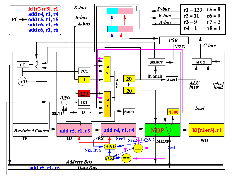
To understand why we use "Dest Reg in IR(WB)" in the test, it is important to pay attention to the location of the LOAD instruction when the fetched value is in the LMDR register.
Take a quick look at the following picture that was from the previous webpage that depicts the situation when the value 4000 was fetched from memory and about to be written to register R1:
The second multiplexor (gold colored one) will select from among: IR1 (a constant), B, ForwReg1 and ForwReg2.
The selection logic of this multiplexor is as follows:
if ( Instruction Imm bit is set to 1 )
select IR1 as operand
else if ( Dest Reg in IR(WB) == Src2 )
select LMDR as operand
else if ( tag1 == Src2 )
select ForwReg1 as operand
else if ( tag2 == Src2 )
select ForwReg2 as operand
else
select B as operand
|
The reason for this test is similar to the first case.
The combinatorial logic of this decision can be formulated as follows:
if ( IR(MEM)'s LD bit == ONE // Load instr in MEM
and IR(EX)'s BRANCH bit == ZERO // ALU, LD or ST instr in EX
and ( IR(EX).Src1 == IR(MEM).Dest
or IR(EX).Src2 == IR(MEM).Dest ) )
then
select STALL EX (and ID) stages
else
select do not stall EX (and ID) stages
|
STALL = (IR(MEM).LoadBit == 1) AND
(IR(EX).BranchBit == 0) AND
( IR(EX).Src1 == IR(MEM).Dest
OR IR(EX).Src2 == IR(MEM).Dest )
LD [R2+R3], R1 R2=11, R3=9, R4=1, R5=8, R6=0, R7=2
ADD R4, R1, R4
ADD R5, R1, R5
ADD R6, R1, R6
ADD R7, R1, R7
...
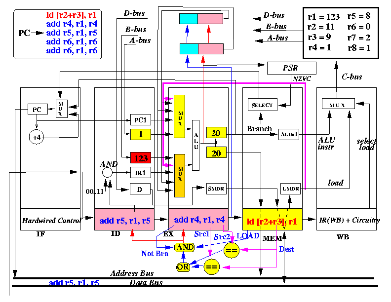
Also, at start of the CPU cycle, the ID stage selects R4 (1) and R1 (123) to be copied into the A and B registers.
Also, at the end of the CPU cycle, the instruction (LD [R2+R3], R1) is moved into IR(MEM), ADD R4, R1, R4 is moved into IR(EX) and instruction ADD R5, R1, R5 is fetched into IR(ID)
The STALL detection hardware will issue a STALL signal to the EX and ID stages
NOTE: the EX stage will perform the normal computation (you can't stop the ALU from doing that and don't need to). At the end, the result of the ALU will simply be ignored and not be used to update the ALUo and LMAR. The most important effect of the stall is the instruction in the EX stage is NOT changed
NOTE: the ID stage will also perform its normal computation - the result fetched from the registers will not be used to update the A and B registers. The most important effect of the stall is the instruction in the ID stage is NOT changed
Also, at the end of the CPU cycle, the instruction (LD [R2+R3], R1) is moved into IR(WB), ADD R4, R1, R4 is RETAINED in IR(EX), instruction ADD R5, R1, R5 is RETAINED in IR(ID)
So the correct value of R1 will be used by the first ADD instruction
That is because the way the general purpose registers are upodated. Recall the timing of the register updates ( click here ):
So the correct value will be fetched (and later used) by the second ADD instruction.
The following picture illustrates what is happening just before the end of the 5th CPU cycle:
I have used the two examples to teach you the principles on how to solve data hazard problems: