Background:
CPU operation (instruction execution cycle)
Review: the CPU repeatedly executes the following in the instruction execution cycle:
|
These steps must be executed in the correct order !!
We will now study how to sequence events using clock signals
Background:
CPU operation (instruction execution cycle)
Review: the CPU repeatedly executes the following in the instruction execution cycle:
|
Accessing the computer memory is a very complex operation.
We will discuss the memory bus protocol later
Background:
CPU operation (instruction execution cycle)
Review: the CPU repeatedly executes the following in the instruction execution cycle:
|
Decoding a machine instruction has be discussed already !!!
The CPU will use the instruction code to control the datapath !!!
In this webpage, I will discuss how to make step 3 happens before step 4
Viewing the CPU as a staged processor
The simplify the discussion, let's consider only the portion of the datapath that connect the registers and the ALU:

The sequencing methodology also applys when MAR and MDR are connected to the datapath.
Viewing the CPU as a staged processor
The datapath circuit is in fact a staged processing circuit:

(Attaching MAR and MDR to this circuit will make it too complex)
Viewing the CPU as a staged processor
Situation: we assume that an instruction has been fetched

How can we perform "fetch operands" before "execute instruction" in chronological order ???
Controlling the
activation time of
components inside the CPU
Reminder: the values stored in memory circuits with only change when they receives a clock signal:

Controlling the
activation time of
components inside the CPU
We fetch the operands first by sending A- & B-buffers a clock signal first:

Controlling the
activation time of
components inside the CPU
We store the result into registers next by sending the destination register a clock signal next:

Controlling the
activation time of
components inside the CPU
Activating timing can be chronologically controlled by using a "N phase clock":

Our CPU will use a 4 phased clock because there are 4 different chronological milestones in the CPU (you will make this circuit in a project).
Controlling the
activation time of
components inside the CPU
Let's activate the components inside the CPU in correct chronological order:

What must happen first in an instruction execution cycle ???
Controlling the
activation time of
components inside the CPU
(1): fetch the next machine instruction and store it in the instruction register (IR):

Phase 1 of the clock happens the earliest of all phases chronologically !!
Controlling the
activation time of
components inside the CPU
The newly fecthed machine instruction will send out control signals:

What must happen next in an instruction execution cycle ???
Controlling the
activation time of
components inside the CPU
(2): fetch the operands from the registers and store them in the A & B-buffers:

Phase 2 of the clock always happens after Phase 1 !!
Controlling the
activation time of
components inside the CPU
Result: we fetch the operands for the fetched instruction in Phase 1 !

What must the CPU update next in an instruction execution cycle ???
Controlling the
activation time of
components inside the CPU
(3): update the MAR using B-buffer data and/or compute with the data in A & B-buffers:

Phase 3 of the clock ensures this happens with correct values inside the A & B-buffers !!!
Controlling the
activation time of
components inside the CPU
Result: (a): MAR=B-buffer and/or (b): the ALU has computed the correct result

What must the CPU update next in an instruction execution cycle ???
Controlling the
activation time of
components inside the CPU
(4): (a): store the result in a register or (b): store the result to memory:

Phase 4 of the clock will ensure that we will use a correctly computed value from the ALU
Controlling the
activation time of
components inside the CPU
The instruction execution cycle is completed and a new cycle starts immediately:

And so on...
Example: controlling the chronological order
of events in
the instruction execution cycle
Suppose the next machine code fetched is 00000000000100010110000000000000:
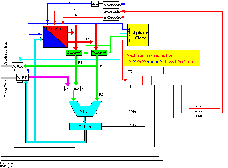
(Ignore the blue colored bits, they are not used to control the CPU operation in this instruction)
Example: controlling the chronological order
of events in
the instruction execution cycle
The first clocking event is the Phase 1 clock signal:
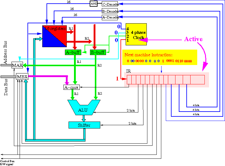
The Phase 1 clock signal will update the IR with the new machine code
Example: controlling the chronological order
of events in
the instruction execution cycle
Result:
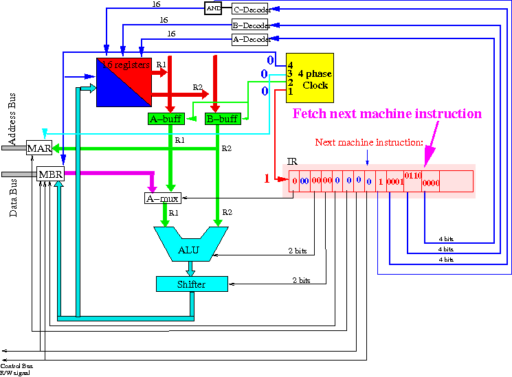
The next clocking event is the Phase 2 clock signal...
Example: controlling the chronological order
of events in
the instruction execution cycle
The new instruction code is sending new selection signal when Phase 2 clock signal occurs:
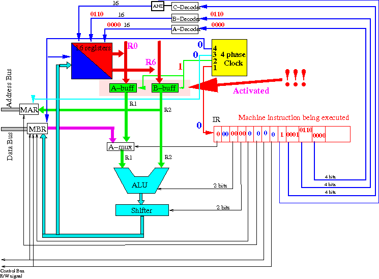
The Phase 2 clock signal will update the A & B-buffers with the values in registers R0 and R6 !
Example: controlling the chronological order
of events in
the instruction execution cycle
Result: the operands (R0 and R6) have been fetched !!!
The next clocking event is the Phase 3 clock signal...
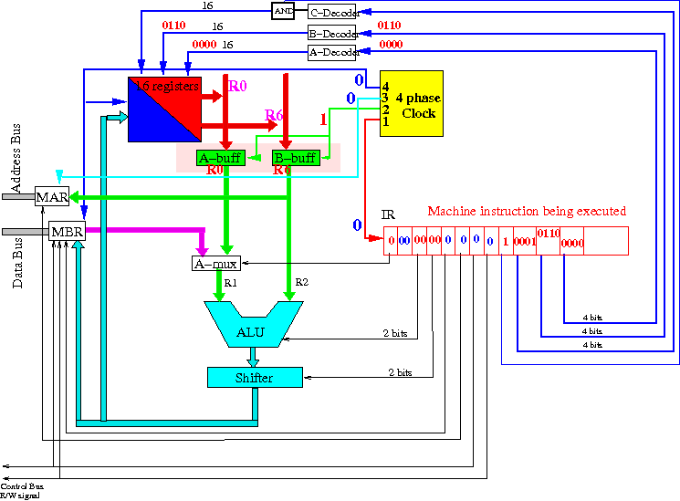
Example: controlling the chronological order
of events in
the instruction execution cycle
During Phase 3, the ALU circuitry will (take time) to compute the sum on the input operands:
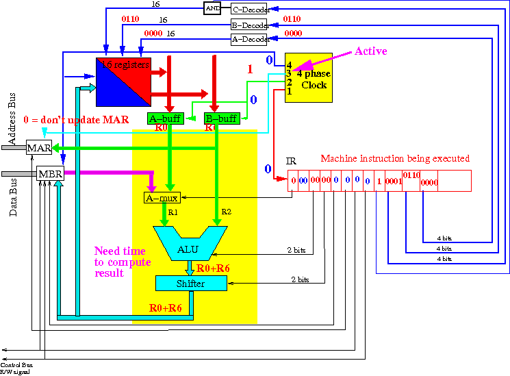
Computational circuits have large delay times (e.g., ripple carry adder !!)
Example: controlling the chronological order
of events in
the instruction execution cycle
Result: at the end of Phase 3 period, the result R0+R6 is on the C-bus:
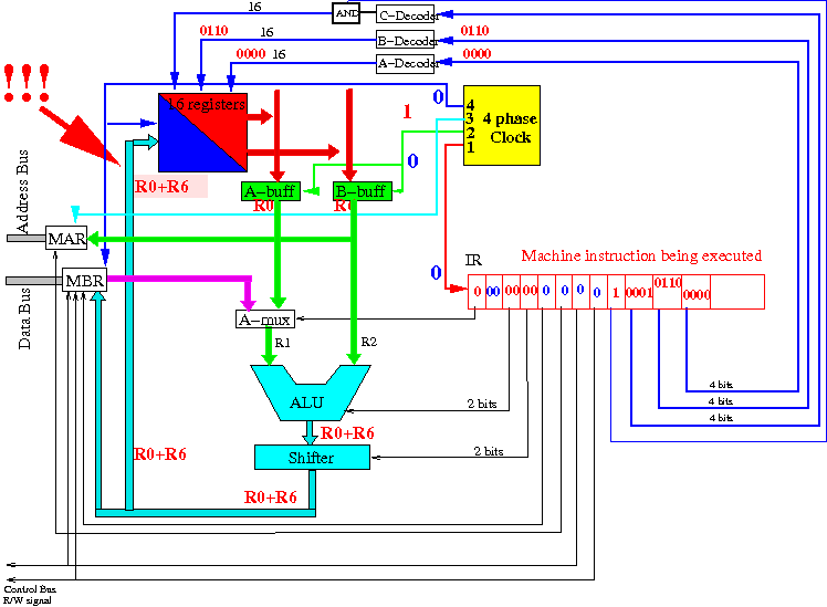
The next clocking event is the Phase 4 clock signal...
Example: controlling the chronological order
of events in
the instruction execution cycle
The Phase 4 clock will update the destination register (R1) with the input value R0+r6:
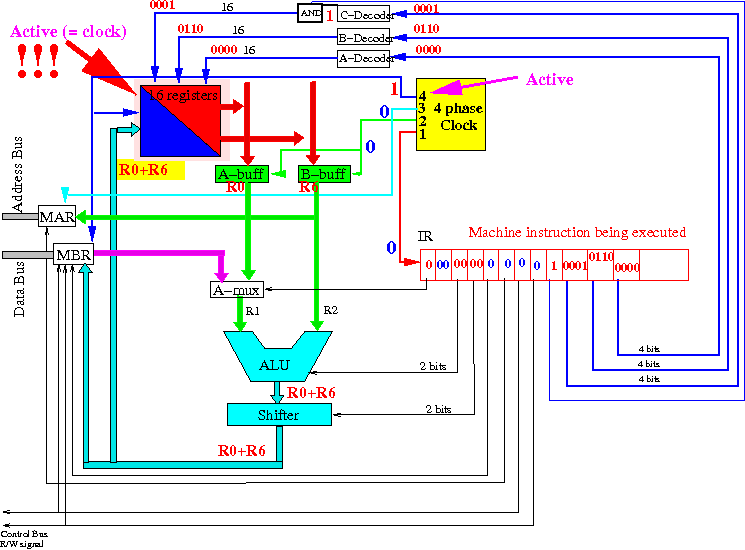
The instruction cycle is completed !!!
Example: controlling the chronological order
of events in
the instruction execution cycle
Result: the CPU has execution the instruction add r1,r0,r6:
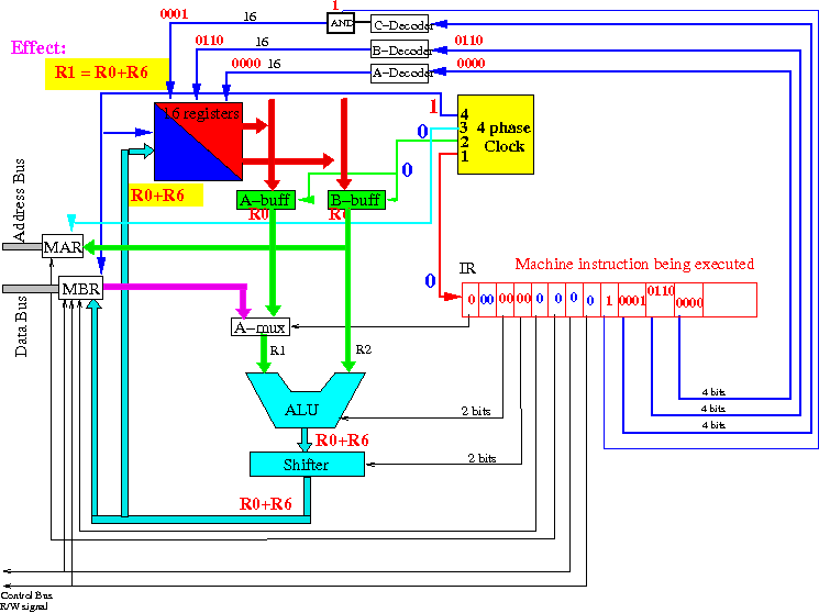
And the instruction execution cycle will repeat again !!!
Example 2: controlling the chronological order
of events in
the instruction execution cycle
Example: the event sequencing in a str machine instruction
We will now look at the event sequences when the CPU executes a str instruction (it's similar)
Example 2: controlling the chronological order
of events in
the instruction execution cycle
Suppose the next machine code fetched is 10010001101000000010000100000000:
(Ignore the blue colored bits, they are not used to control the CPU operation in this instruction)
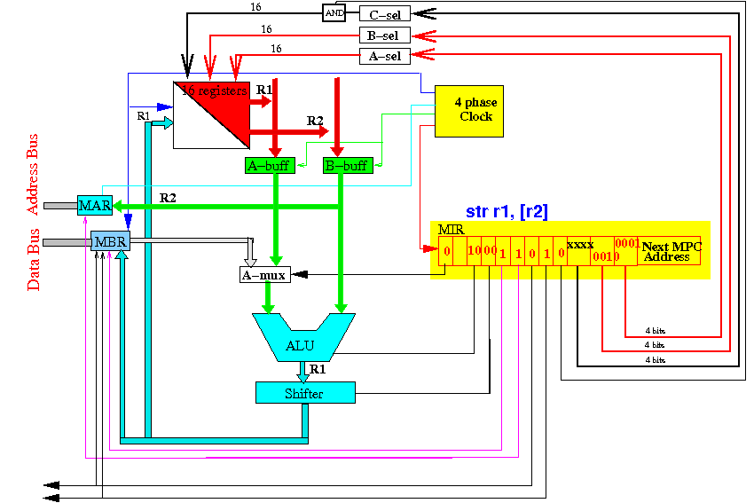
Example 2: controlling the chronological order
of events in
the instruction execution cycle
The first clocking event is the Phase 1 clock signal:
The Phase 1 clock signal will update the IR with the new machine code
Example 2: controlling the chronological order
of events in
the instruction execution cycle
Result:
The next clocking event is the Phase 2 clock signal...
Example 2: controlling the chronological order
of events in
the instruction execution cycle
The new instruction code is sending new selection signal when Phase 2 clock signal occurs:
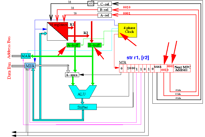
The Phase 2 clock signal will update the A & B-buffers with the values in registers R1 and R2 !
Example 2: controlling the chronological order
of events in
the instruction execution cycle
Result: the operands (R1 and R2) have been fetched !!!
The next clocking event is the Phase 3 clock signal...
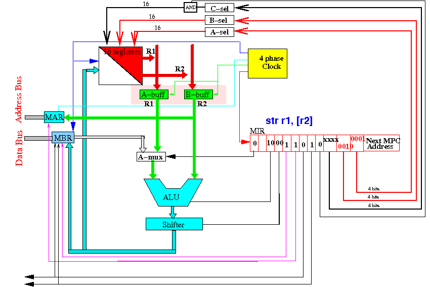
Example 2: controlling the chronological order
of events in
the instruction execution cycle
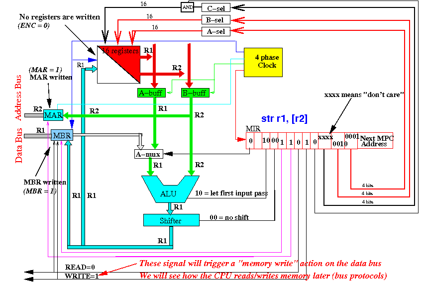
During Phase 3, the ALU + Shifter will compute the R1 and MAR is updated:
The MAR now has the address value (= the value in register R2 !!)
Example 2: controlling the chronological order
of events in
the instruction execution cycle
Result: at the end of Phase 3 period, the R2 is sent on the address bus:
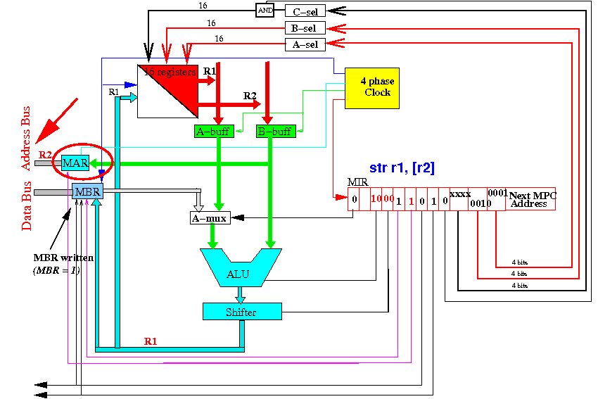
The next clocking event is the Phase 4 clock signal...
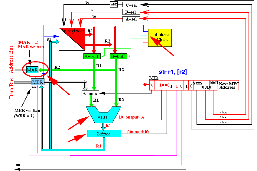
Example 2: controlling the chronological order
of events in
the instruction execution cycle
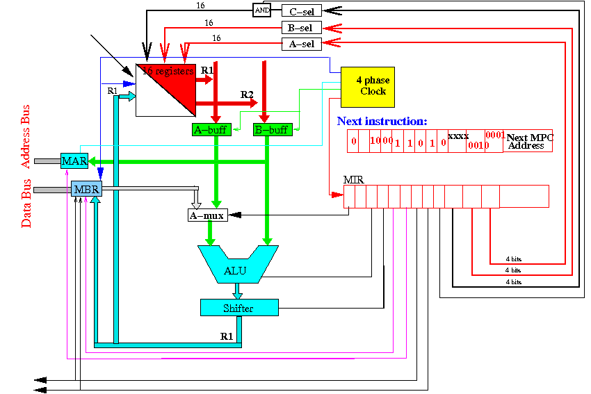
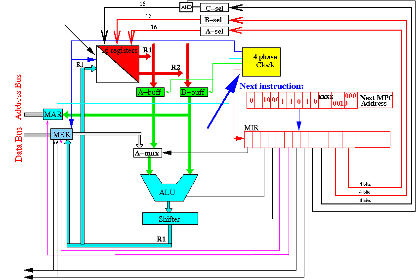
The Phase 4 clock will update the MDR register with the input value R1:
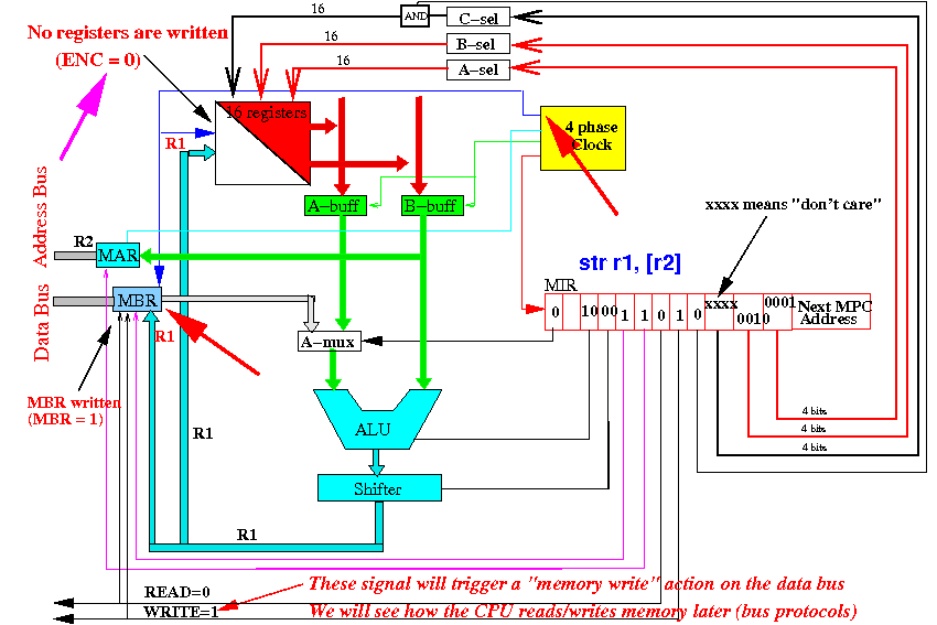
The instruction cycle is completed !!!
Example 2: controlling the chronological order
of events in
the instruction execution cycle
Result: the CPU has executed the instruction str r1,[r2]:
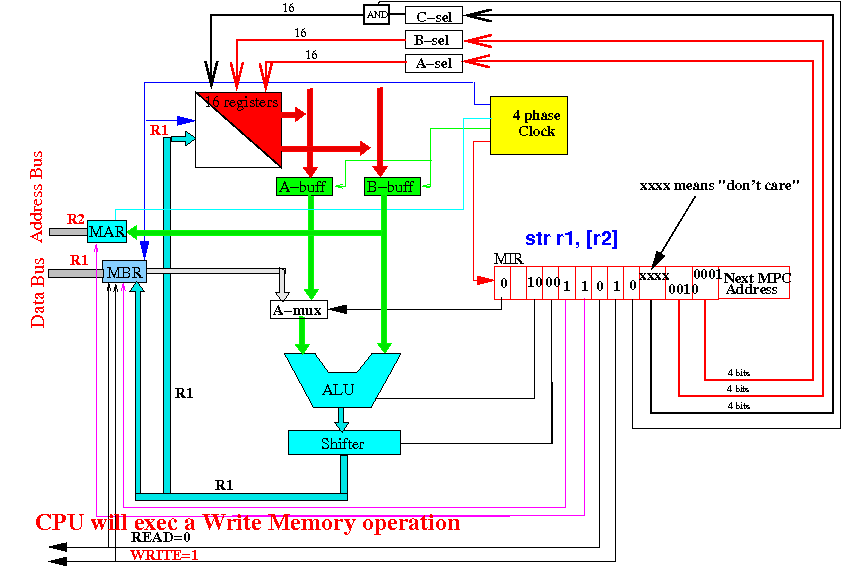
This will trigger the communication subsystem in the CPU to run a "bus protocol" before starting a new instruction execution cycle
DEMO
|
Summary
|