The full adder adds 2 bits together, along with a carry in from the previous bit-addition.
The full adder generate a sum bit and a carry out bit for the next addition stage.
- a, one of the bits to be added
- b, the other bit to be added
- cin, the carry in bit from the previous bit addition
and it has 2 outputs:
- s, the sum bit
- cout, the carry out bit for the next staged bit addition
Schematically:
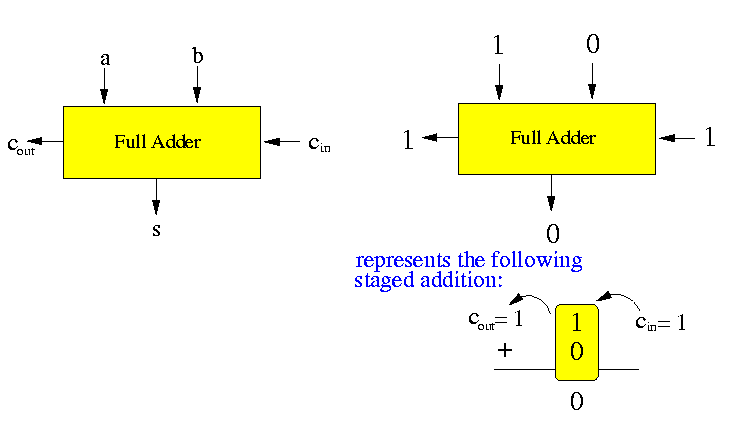
The figure on the right shows the operation of the full adder circuit when it adds the bits 1 and 0, while the previous stage generates a carry (cin = 1).
Here is the boolean function in table form for the adder circuit:
| cin | a | b | cout | s | |
|---|---|---|---|---|---|
| - | - | - | + | - | - |
| 0 | 0 | 0 | 0 | 0 | |
| 0 | 0 | 1 | 0 | 1 | |
| 0 | 1 | 0 | 0 | 1 | |
| 0 | 1 | 1 | 1 | 0 | |
| 1 | 0 | 0 | 0 | 1 | |
| 1 | 0 | 1 | 1 | 0 | |
| 1 | 1 | 0 | 1 | 0 | |
| 1 | 1 | 1 | 1 | 1 |
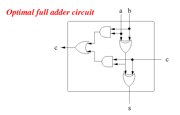
You can see that:
- cout = majority(a, b, cin)
- s = a XOR b XOR c
The optimal full adder circuit is as follows:
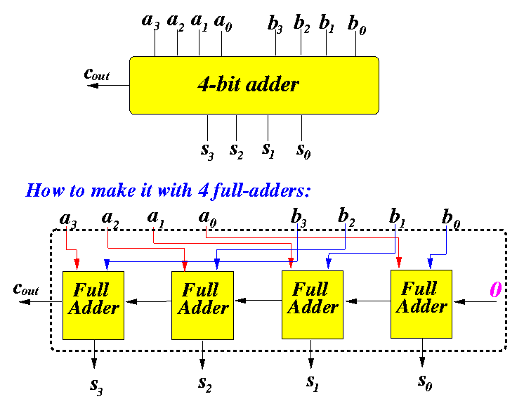
For example, the following circuit will implement a 4-bit adder circuit that can be used to add two 4-bit numbers: